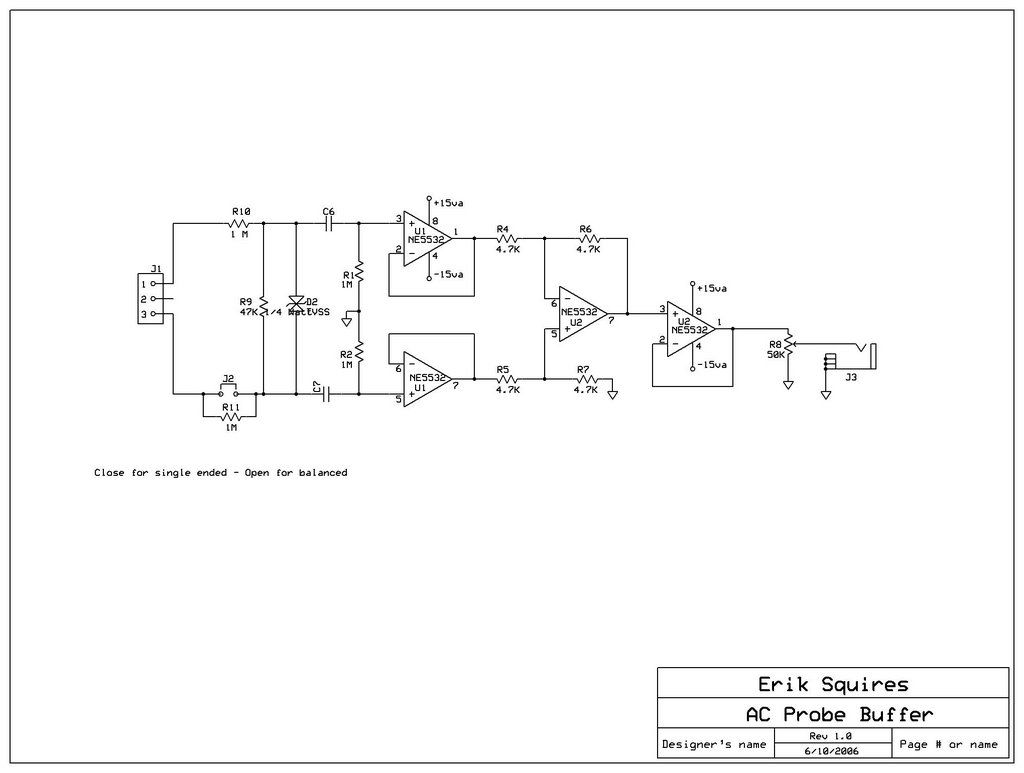
In the interests of full disclosure, I'm including the entire buffer circuit here for your perusal. The first section is a voltage divider which brings the 120 VAC down to a reasonable 5 VAC. There is a shunted 1 MOhm resistor there in case I ever want to compare an isolation transformer or balanced power regenerator a'la PS Audio. The jumper there will be connected to the 115/240 VAC selector switch on the back of the gutted power supply case.
There is also a place for a 15 VAC transient supressing diode made by Littelfuse in case I mess something up, I am hoping this will keep me from frying the laptop. After this, there are two 250VAC 0.1uF metal fil caps which couple the input stage to the amplifier buffer stage itself.
The buffer stage consists of NE5532 Op-Amps for several reasons. I have them, they are relatively low noise and low distortion, and they can directly drive a 600 Ohm load. In the circuit board design I was going to switch over to a single quad J-FET op-amp, the TL072, which are low noise but in the breadboard prototype I noticed some odd voltage drops when connecting the buffer to the mic input. This made me worry more about the mic input impedance than before.
Now, in an ideal situation, I would use a transformer of some sort to keep the current on the input side of the buffer from finding a way through ground to the neutral. However, good signal level transformers such as those made by Jensen Transformers are pricey, and I no longer have the room to put one in the board. Good thing they decided not to sponsor me, because I would have had to get a bigger circuit board. :)
The power supply is not shown, but it involves the salvaged bridge rectifier from the PC supply, 4x2,200 uF Panasonic FM caps feeding LM78L15 and LM79L15 voltage regulators, after which are a pair of 4.7uF tantalum caps, and perhaps a pair of 0.1uF metal film caps as well.
The last part of the buffer is a multi-turn pot. The mic input only accepts signals between +- 1 Volt. The buffer circuit is set to a gain of 1. So, becasue of this, the signal must be reduced from 5 Volts RMS on the output of the buffer to less than 1 Volt RMS on the Cardas RCA jack. When using a balanced input, I'll have to turn this back up a little.
The good news is that because there is so much attenuation, what little noise and ripple are in the op-amp outputs they get reduced by a factor of about 5, so I expect that my overall SNR will be quite high. I certainly can't see it in the scope measurements.
Before anyone goes nuts asking me why I didn't use this part or that, remember two things. First, I'm on a very tight budget. Second, I'm looking for relative differnces in performance of power conditioners. The normal THD+N measurement at my desk of the AC line is about 7%. Not 0.7%, but 7%! Probably two orders of magnitude greater than the buffer circuit I'm using. Also, I don't want to accidentally clean up the signal by putting too much in the circuit. The one exception I've made to this are fuses and a TVSS to keep me from frying anything. But the TVSS is off until it's overloaded.
No comments:
Post a Comment